¶ Screen Test
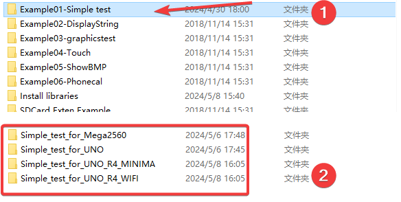
This test program verifies the integrity of the display screen and screens for dead pixel defects. Multiple versions of sample codes are provided for selection based on your equipped microprocessor model.
¶ Code Explanation
The sample code demonstrated here is based on Arduino UNO R3. The operation logic of other microcontrollers is roughly the same, with only minor differences in the code for Arduino UNO R4.
¶ Pin Definition Description
- Data Pin Mapping (Hardware Fixed)
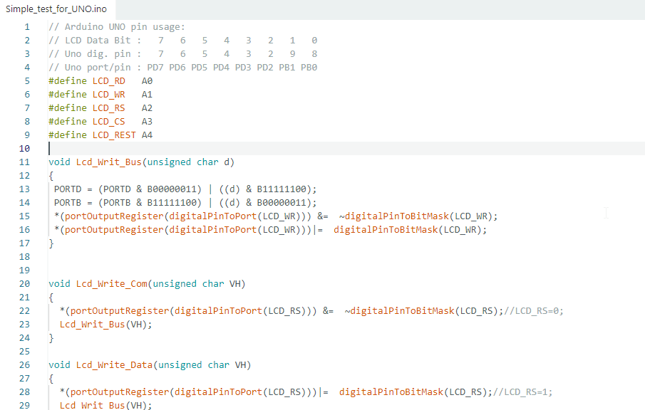
The LCD data pins D7 to D0 of the screen adopt fixed hardware mapping. They correspond to pins 7, 6, 5, 4, 3, 2, 9 and 8 of the Arduino board in sequence, and the corresponding single-chip microcomputer registers are PD7, PD6, PD5, PD4, PD3, PD2, PB1 and PB0 respectively. The mapping of hardware pins and registers cannot be modified manually.
// Arduino UNO pin usage:
// LCD Data Bit :   7   6   5   4   3   2   1   0
// Uno dig. pin :   7   6   5   4   3   2   9   8
// Uno port/pin : PD7 PD6 PD5 PD4 PD3 PD2 PB1 PB0
- Control Pin Macro Definition
The following macro definitions are uniformly adopted in this document to configure the screen control pins for Arduino main control boards:
#define LCD_RD   A0
#define LCD_WR   A1
#define LCD_RS   A2
#define LCD_CS   A3
 #define LCD_REST A4
- Pin Function Description
The core functions of each control pin are described as follows:
- LCD_RS: Instruction and data selection pin, used to switch the working mode of the screen between instruction input and data transmission.
- LCD_WR: Data write trigger pin, which triggers the screen to perform data write operations.
- LCD_CS: Chip select enable pin, used to activate and select the current display device.
- LCD_REST: Display reset pin, used to perform hardware reset on the display screen.
¶ Description of Carry Bit Operation
- Bitwise AND (&)
Rule: The result bit is 1 only when both corresponding bits are 1; otherwise, the result bit is 0.
Function: Clears designated bits and retains target bits to achieve accurate data filtering.
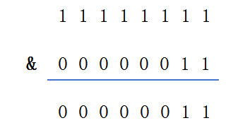
Example: Calculate PORTD & B00000011
Original port state: PORTD = 0b11111111
Effect: Accurately retains the lowest 2 bits of the port and forcibly clears the upper 6 bits, providing a clean foundation for subsequent high-bit data writing.
- Bitwise OR (|)
Rule: The result bit is 1 if either of the corresponding bits is 1; the result bit is 0 only when both bits are 0.
Function: Splicing two sets of binary data. It retains the original low-bit state and fills in new high-bit data to avoid overwriting the original port state.
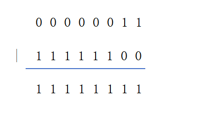
Example: Splice the retained original port data and new high-bit data
Retained old bits = 0b00000011, New high-bit data = 0b11111100
Effect:Realizes seamless splicing of old and new data. It preserves the original pin status while writing new data correctly, completing accurate port assignment.
- Bitwise NOT (~)
Rule: Inverts each binary bit: 0 becomes 1, and 1 becomes 0.
Function: Precisely flips the level state of the specified pin without affecting other pins on the port.
Example: In this code, the mask of the WR pin is 0b00000010. The bitwise operation ~0b00000010 outputs 0b11111101. Combined with bitwise AND operation, only the WR pin is cleared, and all other port pins remain unchanged.
¶ Detailed Explanation of Underlying Core Functions
¶ Lcd_Writ_Bus()
This function is the underlying core function of the LCD driver. It splits 1-byte (8-bit) data and outputs it in parallel to 8 LCD data pins. Meanwhile, it generates a WR rising-edge pulse to trigger the LCD to latch data and complete single-byte data reception.
void Lcd_Writ_Bus(unsigned char d)
{
 PORTD = (PORTD & B00000011) | ((d) & B11111100);
 PORTB = (PORTB & B11111100) | ((d) & B00000011);
 *(portOutputRegister(digitalPinToPort(LCD_WR))) &=  ~digitalPinToBitMask(LCD_WR);
 *(portOutputRegister(digitalPinToPort(LCD_WR)))|=  digitalPinToBitMask(LCD_WR);
}
- High 6-bit data assignment: PORTD = (PORTD & B00000011) | ((d) & B11111100);
This statement accurately updates the high 6-bit data of the PORTD port through bitwise operations, while retaining the original state of the port’s low 2 bits to prevent irrelevant pin states from being modified.
- PORTD & B00000011: Clears the high 6 bits (PD2~PD7) of the PORTD port and only retains the original state of the lowest 2 bits.
- d & B11111100: Masks the low 2 bits of the incoming byte data and extracts only the valid high 6-bit data.
- Bitwise OR splicing: Splices the retained original low-bit state of the port with the new high-bit data to complete the output of high 6-bit data on the LCD bus.
- Low 2-bit data assignment: PORTB = (PORTB & B11111100) | ((d) & B00000011);
This statement updates the low 2-bit data of the PORTB port and keeps the original state of the port’s high 6 bits, completing the output of the remaining data of the single-byte value.
- PORTB & B11111100: Clears the low 2 bits (PB0, PB1) of the PORTB port and retains the state of the high 6 bits.
- d & B00000011: Masks the high 6 bits of the incoming byte data and extracts only the valid low 2-bit data.
- Bitwise OR splicing: Combines the original high-bit state of the port with the new low-bit data to complete the full 8-bit data output.
- Pull down WR pin:
*(portOutputRegister(digitalPinToPort(LCD_WR))) &= ~digitalPinToBitMask(LCD_WR);
Combines bitwise NOT and bitwise AND operations to pull down the level of the LCD_WR pin independently without affecting other pins, preparing the timing for data writing. - Pull up WR pin: *(portOutputRegister(digitalPinToPort(LCD_WR))) |= digitalPinToBitMask(LCD_WR);
Pulls up the LCD_WR pin level via bitwise OR operation to generate a standard rising-edge pulse. This triggers the LCD hardware to latch the 8-bit data on the bus and finish single-byte data writing.
¶ Lcd_Write_Com()
This dedicated underlying function is used to send control commands to the LCD display. It can complete core control operations including screen parameter configuration, working mode switching, function enabling and resetting, and serves as the basic command interface for all LCD driver functions.
void Lcd_Write_Com(unsigned char VH)
{
  *(portOutputRegister(digitalPinToPort(LCD_RS))) &=  ~digitalPinToBitMask(LCD_RS);//LCD_RS=0;
  Lcd_Writ_Bus(VH);
}
- Function Entry: void Lcd_Write_Com(unsigned char VH)
Defines the LCD command writing function. The input parameter VH is an 8-bit unsigned char, which is used to receive LCD register command codes (0~255). All screen operations such as parameter configuration, function switching and reset are passed through this parameter. - Pull down RS pin:
*(portOutputRegister(digitalPinToPort(LCD_RS))) &= ~digitalPinToBitMask(LCD_RS);
This is a low-level register operation for Arduino, which runs faster than common pin control functions. The detailed breakdown is as follows:
- digitalPinToPort(LCD_RS): Obtains the physical port address corresponding to the custom LCD_RS pin;
- portOutputRegister(): Acquires the output register address of the port and directly controls hardware pins through pointers;
- digitalPinToBitMask(LCD_RS): Generates a unique bit mask to locate the target RS pin;
- Bitwise NOT (~): Inverts the bit mask, sets the target pin bit to 0 and all other bits to 1;
- Bitwise AND assignment (&=): Clears only the LCD_RS pin level while completely retaining the status of other pins on the same port without interference.
Core Function: Complies with the standard LCD 8080 parallel communication protocol. RS=0 represents command mode, telling the LCD that the currently transmitted content is a control command instead of display data.
- Bus Data Transmission: Lcd_Writ_Bus(VH);
Calls the encapsulated underlying bus transmission function. It outputs the 8-bit command code stored in parameter VH to the LCD through the D0~D7 8-bit parallel data bus.
This function automatically completes all underlying operations: data bit splitting, stable bus output, WR rising-edge pulse generation, and LCD hardware command latching, finally completing the writing and execution of a single screen command.
¶ Lcd_Write_Data()
This dedicated underlying function is used to send display data to the LCD, including pixel color data and coordinate positioning data. It serves as the core underlying interface for screen dotting, area filling, character display and graphic drawing. Cooperating with the bus driver function, it completes all hardware writing operations of screen display data.
void Lcd_Write_Data(unsigned char VH)
{
  *(portOutputRegister(digitalPinToPort(LCD_RS)))|=  digitalPinToBitMask(LCD_RS);//LCD_RS=1;
  Lcd_Writ_Bus(VH);
}
- Function Entry: void Lcd_Write_Data(unsigned char VH)
Defines the LCD display data writing function. The input parameter VH is an 8-bit unsigned char, which receives all display-related byte data such as pixel color values, coordinate offset data and screen filling data, with a value range of 0~255. - Pull up RS pin:
*(portOutputRegister(digitalPinToPort(LCD_RS))) |= digitalPinToBitMask(LCD_RS);
This code adopts direct low-level register operation for Arduino, which is more efficient than ordinary pin control functions. It only changes the state of the RS pin without affecting other pins on the same port. The detailed breakdown is as follows:
- digitalPinToPort(LCD_RS): Reads the physical hardware port address corresponding to the custom LCD_RS pin;
- portOutputRegister(): Obtains the output register address of the port and directly controls hardware pins through pointers for high-speed underlying operation;
- digitalPinToBitMask(LCD_RS): Generates a unique bit mask to accurately locate the RS pin;
- Bitwise OR assignment (|=): Performs bitwise OR operation on the port register and pin mask to pull up only the LCD_RS pin and keep all other pin states unchanged.
Core Function: Complies with the standard LCD 8080 parallel communication protocol. RS=1 represents data mode, informing the LCD that the currently transmitted content is display data rather than control commands, and switching the LCD to data receiving state.
- Bus Data Transmission: Lcd_Writ_Bus(VH);
Calls the encapsulated general underlying bus transmission function to output the 8-bit display data stored in parameter VH to the LCD through the D0~D7 8-bit parallel data bus.
This function automatically completes underlying hardware logic, including 8-bit data splitting, stable port data locking and WR rising-edge pulse generation. Finally, the LCD hardware latches the bus data to complete single display data writing and support screen lighting and image refreshing.
Overall Timing Logic
Independently pull up the RS pin to switch to display data mode → Stably output 8-bit pixel/coordinate data to the data bus → Generate WR rising-edge pulse → The LCD latches display data and refreshes the corresponding screen area to complete single display data writing.
¶ Lcd_Write_Com_Data()
This function is a combined encapsulated function dedicated to LCD register configuration. It simplifies the driver code by completing the full operation of "writing functional commands + writing corresponding configuration data" in one call. It is applicable to most register parameter configuration scenarios of LCD screens and serves as a commonly used quick interface for screen initialization and parameter configuration.
void Lcd_Write_Com_Data(unsigned char com,unsigned char dat)
{
  Lcd_Write_Com(com);
  Lcd_Write_Data(dat);
}
¶ Address_set()
This function locks a specified rectangular drawing area on the screen. After the area is set, all subsequent color data will only be filled within the defined region. It is the underlying basis for screen clearing, line drawing and graphic rendering.
void Address_set(unsigned int x1,unsigned int y1,unsigned int x2,unsigned int y2)
{
   Lcd_Write_Com(0x2a);
    Lcd_Write_Data(x1>>8);
    Lcd_Write_Data(x1);
    Lcd_Write_Data(x2>>8);
    Lcd_Write_Data(x2);
   Lcd_Write_Com(0x2b);
    Lcd_Write_Data(y1>>8);
    Lcd_Write_Data(y1);
    Lcd_Write_Data(y2>>8);
    Lcd_Write_Data(y2);
    Lcd_Write_Com(0x2c);
}
- 0x2a: X-axis coordinate setting command. It writes the X-axis start point and end point coordinates in sequence. The >>8 (8-bit right shift) operation splits 16-bit coordinate data into high 8 bits and low 8 bits for separate transmission.
- 0x2b: Y-axis coordinate setting command. It follows the same principle as the X-axis to set the Y-axis start and end coordinate range.
- 0x2c: Enables video memory write mode. After the rectangular area is locked, the screen waits for incoming pixel data, and all subsequent data will be filled into the preset drawing area.
¶ Lcd_Init()
This function completes hardware reset and full register parameter configuration for the LCD. It wakes up the screen and configures parameters such as operating voltage, color format and refresh rate to make the screen enter a normal display state.
void Lcd_Init(void)
{
  digitalWrite(LCD_REST,HIGH);
  delay(5);
  digitalWrite(LCD_REST,LOW);
  delay(15);
  digitalWrite(LCD_REST,HIGH);
  delay(15);

  digitalWrite(LCD_CS,HIGH);
  digitalWrite(LCD_WR,HIGH);
  digitalWrite(LCD_CS,LOW);

    // Bottom-level timing, voltage and gain configuration commands
    Lcd_Write_Com(0xCB);
    Lcd_Write_Data(0x39);
    Lcd_Write_Data(0x2C);
    Lcd_Write_Data(0x00);
    Lcd_Write_Data(0x34);
    Lcd_Write_Data(0x02);

    Lcd_Write_Com(0xCF);
    Lcd_Write_Data(0x00);
    Lcd_Write_Data(0XC1);
    Lcd_Write_Data(0X30);

    Lcd_Write_Com(0xE8);
    Lcd_Write_Data(0x85);
    Lcd_Write_Data(0x00);
    Lcd_Write_Data(0x78);

    Lcd_Write_Com(0xEA);
    Lcd_Write_Data(0x00);
    Lcd_Write_Data(0x00);

    Lcd_Write_Com(0xED);
    Lcd_Write_Data(0x64);
    Lcd_Write_Data(0x03);
    Lcd_Write_Data(0X12);
    Lcd_Write_Data(0X81);

    Lcd_Write_Com(0xF7);
    Lcd_Write_Data(0x20);

    Lcd_Write_Com(0xC0); // Power control
    Lcd_Write_Data(0x23);

    Lcd_Write_Com(0xC1); // Power control
    Lcd_Write_Data(0x10);

    Lcd_Write_Com(0xC5); // Contrast control
    Lcd_Write_Data(0x3e);
    Lcd_Write_Data(0x28);

    Lcd_Write_Com(0xC7); // Brightness control
    Lcd_Write_Data(0x86);

    Lcd_Write_Com(0x36); // Scan direction configuration
    Lcd_Write_Data(0x48);

    Lcd_Write_Com(0x3A); // Color format configuration
    Lcd_Write_Data(0x55);

    Lcd_Write_Com(0xB1); // Refresh rate configuration
    Lcd_Write_Data(0x00);
    Lcd_Write_Data(0x18);

    Lcd_Write_Com(0xB6); // Display function configuration
    Lcd_Write_Data(0x08);
    Lcd_Write_Data(0x82);
    Lcd_Write_Data(0x27);

    Lcd_Write_Com(0x11); // Exit sleep mode
    delay(120);

    Lcd_Write_Com(0x29); // Enable screen display
    Lcd_Write_Com(0x2c);
}
- Reset timing: Switch the REST pin through high-low-high level with delay stabilization to complete LCD hardware reset.
- Pin initialization: Pull up CS and WR pins by default, then pull down the CS pin to select the current display screen.
- Command group 0xCB~0xF7: Configure screen clock, driving voltage and timing gain to fix screen flickering and abnormal display.
- Command group 0xC0~0xC7: Configure screen power supply, display contrast and brightness parameters.
- Command 0x36: Set forward screen scanning mode and disable screen mirror flipping.
- Command 0x3A: Configure the screen to RGB565 16-bit color format.
- Command 0xB1 and 0xB6: Set screen refresh rate and pixel scanning mode.
- Command 0x11: Make the screen exit sleep mode, and delay 120ms for hardware initialization completion.
- Command 0x29 and 0x2C: Light up the screen and enable normal display and video memory writing functions.
¶ H_line()
This function draws a horizontal line with specified length and color at the screen coordinate (x, y). It is a basic core function for screen graphic rendering.
void H_line(unsigned int x, unsigned int y, unsigned int l, unsigned int c)
{
  unsigned int i,j;
  Lcd_Write_Com(0x02c); //write_memory_start
  digitalWrite(LCD_RS,HIGH);
  digitalWrite(LCD_CS,LOW);
  l=l+x;
  Address_set(x,y,l,y);
  j=l*2;
  for(i=1;i<=j;i++)
  {
    Lcd_Write_Data(c);
  }
  digitalWrite(LCD_CS,HIGH);
}
- Command 0x02c: Manually enables the screen video memory write mode to prepare for pixel drawing.
- Pin configuration: Pull up the RS pin and pull down the CS pin to enter data write mode and select the current screen.
- Coordinate calculation: Calculate the X-axis end coordinate of the horizontal line by adding the line length to the starting X coordinate, and call the coordinate setting function to lock the horizontal drawing area.
- Cyclic color filling: Writes the specified color data in a loop to continuously light up a row of pixels and generate a solid-color horizontal line.
¶ V_line()
This function draws a vertical line with specified length and color at the screen coordinate (x, y). As a core basic graphics rendering function, it supports cooperative use with the horizontal line drawing function.
void V_line(unsigned int x, unsigned int y, unsigned int l, unsigned int c)
{
  unsigned int i,j;
  Lcd_Write_Com(0x02c); //write_memory_start
  digitalWrite(LCD_RS,HIGH);
  digitalWrite(LCD_CS,LOW);
  l=l+y;
  Address_set(x,y,x,l);
  j=l*2;
  for(i=1;i<=j;i++)
  {
    Lcd_Write_Data(c);
  }
  digitalWrite(LCD_CS,HIGH);
}
¶ Rectf()
This function draws a solid filled rectangle with a single color. Taking the screen coordinate (x, y) as the top-left starting point, it fills the entire rectangular area with the specified color according to the defined width w and height h. It is a basic function for screen clearing and color block display.
void Rectf(unsigned int x,unsigned int y,unsigned int w,unsigned int h,unsigned int c)
{
  unsigned int i;
  for(i=0;i<h;i++)
  {
    H_line(x  , y  , w, c);
    H_line(x  , y+i, w, c);
  }
  }
- Define the loop variable i for longitudinal offset traversal of the rectangle height.
- The for loop iterates according to the rectangle height h to cover the entire vertical range of the rectangle.
- The horizontal line drawing function is called cyclically. The Y-axis coordinate is offset dynamically by the loop variable i, and solid-color horizontal lines are drawn row by row from top to bottom.
- All horizontal lines are stacked vertically without gaps, completely covering the rectangular area and realizing solid color filling.
¶ RGB()
This dedicated color conversion function converts conventional 8-bit R, G, and B brightness values into standard 16-bit RGB565 color codes adapted for LCD screens. It provides standardized color data for all graphics drawing functions.
int RGB(int r,int g,int b)
{return r << 16 | g << 8 | b;
}
1.r << 16: Red component 16-bit left shift
Shifts the 8-bit red brightness data 16 binary bits to the left. The red component occupies the high-bit area of the 16-bit color value and reserves low-bit space for green and blue components.
2. g << 8: Green component 8-bit left shift
Shifts the 8-bit green brightness data 8 binary bits to the left. The green component fills the middle-bit area to realize layered occupation of three primary colors.
3. Bitwise OR splicing
The bitwise OR operation seamlessly combines the shifted red, green and blue components. It merges separate 8-bit three-color data into a complete set of 16-bit RGB565 color codes recognizable by the LCD screen.
Core Principle: Left shift operations layer and occupy bit positions for each color component. Combined with lossless bitwise OR data splicing, general RGB values are standardized into 16-bit pixel color data directly supported by the LCD driver.
¶ LCD_Clear()
This underlying full-screen clearing function fills the entire 240*320 resolution LCD screen with a specified solid color. It is widely used in interface initialization, screen refreshing and display reset, serving as a basic core function for screen interface updating.
void LCD_Clear(unsigned int j)
{
  unsigned int i,m;
  Address_set(0,0,240,320);
  digitalWrite(LCD_CS,LOW);

  for(i=0;i<240;i++)
    for(m=0;m<320;m++)
    {
      Lcd_Write_Data(j>>8);
      Lcd_Write_Data(j);
    }
  digitalWrite(LCD_CS,HIGH);
}
- Define loop variables i and m for double-loop traversal of all pixel rows and columns on the screen.
- Address_set(0,0,240,320): Locks the full display area of the screen, starting from coordinate (0,0) and ending at (240,320), limiting subsequent color data to fill the entire screen range.
- digitalWrite(LCD_CS,LOW): Pulls down the chip select pin level to select the current LCD screen and enable data writing permission.
- Double for-loop: The outer loop traverses screen pixel rows, and the inner loop traverses screen pixel columns, covering all pixels of the screen.
- j>>8 data splitting and transmission: The screen adopts 16-bit RGB565 color format. The 16-bit color value is split by an 8-bit right shift operation. The high 8-bit color data is transmitted first, followed by the low 8-bit data, which complies with the standard LCD color rendering protocol to complete single pixel coloring.
- After the loop ends, pull up the CS pin to disable screen chip selection and terminate the full-screen filling operation.